DIRECT ETCH PAGE

© copyright 2003 LKG Industries Inc.
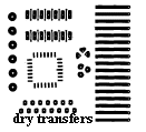
What is DIRECT ETCH? Also referred to as "DE", the product group consists of patterns that can be rubbed down (burnished) onto either a copper laminated PC board, or onto clear film or paper to create a PC board circuit pattern. These patterns are "dry-transfers" that provide not only tidy donut pads for component leads but, more important, provide exact spacing that will match the IC’s, transistors and other components that you will use in your electronic circuit.
Why DIRECT ETCH? Creating a simple
circuit is fast and easy using DE. If you don’t have a particularly good
computer with expensive circuit creating software, DE can be a fast and easy
alternative. DE cost will be very little when compared to using a computer.
Practiced users go way beyond ‘simple’ circuit; making layouts (artwork) for
large, involved circuits.
DE patterns may be applied directly to the copper surface and
then the board may be etched with the DE patterns acting as etch resist. Perfect
PC boards can result!
Or, DE patterns may be applied to clear film or paper to make
a "positive" so that you can make many copies of your circuit. Use your positive
with DATAK Premier® PC boards.

When you have placed the patterns and pads, they can be
connected either with dry-transfer lines or use thin black tape, available from
DATAK. The tape, much like a very narrow and black masking tape, can be applied
to a drawing or on copper to resist etching. Many widths are available and shown
in a chart on this page.
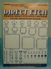
If you want to try DE, beginning with a kit is a good way to start.
![]()
DIRECT ETCH® KITS
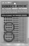
The no. ER-2 kit contains 8 sheets of patterns in a mixed assortment (good for most small circuits) and two rolls of the DE tape, one 1/16" and one 1/32" wide. Includes patterns for IC’s and plenty for resistors, diodes, capacitors and other two-lead components. And, it’s easy to use the included patterns to make PC board patterns for ‘odd’ components too.
Order part no. ER-2 Kit
![]()
COMPLETE DE® PRINTED CIRCUIT KIT (click photo for larger view)
The DATAK no. ER-1 contains
everything needed to make some small circuit. Included: several copper clad PC
boards, large assortment of DE patterns including DIP’s, donuts, transistor
patterns as well as lines and tape. There are four (4) boards, and enough
etchant concentrate to etch them. The plastic display case acts as an etching
tray.
You will need to add a glass or plastic pint bottle to mix
and store the etchant. And, you’ll need something like a Popsicle stick to
burnish down the patterns (a wide tip ballpoint pen may be used, avoid the fine
tip size).
![]()
This is the kit to buy if you
have tried one of the kits above and know that you will likely be making a
number of circuits; this is a very comprehensive and in-depth assortment.
Included are donut pads, SMD footprints and hundreds of patterns to match
industry standard components. Use these patterns on copper or on film for
producing more than one PC board.
When using on clear film, use DATAK 12-500 film and you may
want to place a 1/10" grid under the film to guide donut placements. DATAK grid
sheets are no. 12-505.
Finally, you need to consider a good burnishing tool and a "hobby knife" to make the job easier. These item are shown below.
![]()
BURNISHING TOOLS
A quality burnishing tool
will be a lot easier to use than trying to fake it with a Popsicle stick or a
bold ballpoint pen. When tackling serious circuit layouts, we strongly recommend
the no. 04158 tool.

Part no. 04158 A quality burnishing tool with a polished metal tip. (top photo, click to enlarge)
Part no. 04159 Spoon Tip Burnish tool is intended for use with large
patterns, lettering that is above 1/4" in size and other large jobs. Not necessarily needed for average PC board work;
suggested for use if you will be using large lettering; and can be handy when
using DATAK panel marking Dry-transfers. (bottom photo)
![]()
GOT Etchant? look on the DATAK Positive products page.
© copyright 2003 LKG Industries Inc.
